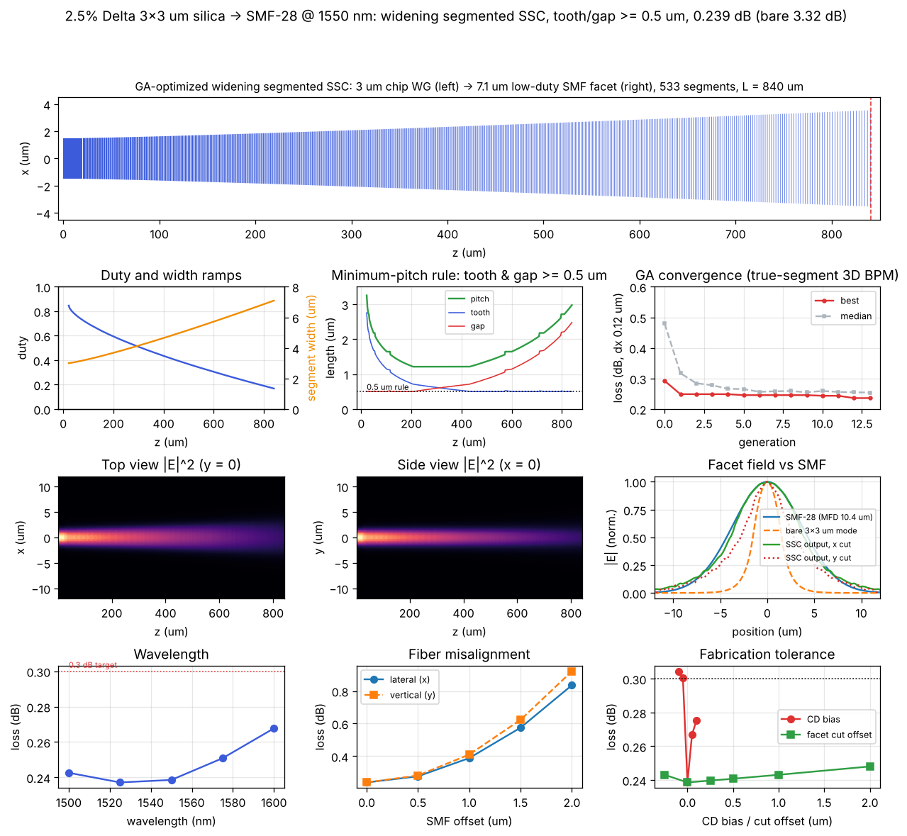
2.5% Δ silica channel waveguide (3×3 µm) ↔ SMF-28 at 1550 nm — segments that gradually widen on the narrowest pitch the mask rule allows (every tooth and gap ≥ 0.5 µm), optimized with a genetic algorithm driving a 3D BPM through the real tooth/gap geometry. Coupling loss 0.239 dB.
Target & SMF parameters
The last field is the mode-field diameter the SSC facet presents to the SMF (the optimized device delivers ≈ 11.5 × 10.0 µm, geometric mean ≈ 10.7 µm). Set it equal to the bare WG MFD to see the loss without a converter.
n_core (from Δ)
—
n_clad (silica, Sellmeier)
—
Bare WG mode field diameter (D4σ)
—
Coupling loss — bare WG ↔ SMF
—
Coupling loss — SSC tip ↔ SMF
—
Improvement
—
SSC quality
—
Gaussian–Gaussian overlap model for a quick estimate; the reported design numbers below come from the true-segment 3D BPM.
Mode field cross-section — blue: SMF Gaussian, red dashed: bare WG mode, green: expanded SSC-tip mode. Larger overlap with the SMF means lower loss.
Why a spot size converter
The SMF-28 mode-field diameter is ~10.4 µm at 1550 nm, while a 2.5% Δ, 3×3 µm silica core guides only a 3.9 µm (D4σ) mode — the bare butt-coupling loss is 3.32 dB.
The 3 µm core thickness is fixed by deposition, so the converter must be drawn in the mask plane only: segment width and duty lower the local effective index and let the mode swell in both x and y.
At 2.5% Δ every gap is a strong scatterer. A coarse fixed pitch (e.g. 2.8 µm) adds ~0.5 dB of segment radiation, so the pitch is kept as short as the 0.5 µm rule allows wherever the duty is mid-range — and the segments widen gradually so the facet mode is large without pushing the duty to the rule limit too early.
Target: SMF coupling loss ≤ 0.3 dB, minimum linewidth / gap ≥ 0.5 µm.
Structure & design variables
Chip waveguide 3 µm solid (20 µm lead) → segmented section whose segments widen from 3 µm toward the SMF facet while their duty falls. Each period starts with a gap, then a tooth; the facet is cut at the end of the last tooth. The segment list is generated from a small gene vector:
Global pitch floor (above the 2nd-order Bragg band)
1.15 – 1.50 µm
1.21 µm
Local pitch rule: Pk = max( P_min , 0.5 µm / (1 − d) , 0.5 µm / d ) → nudged out of the Bragg bands m·λ / (2 neff), m = 2…6 (±0.03 µm guard)
So the gap is pinned at 0.5 µm near the chip (high duty), the pitch drops to P_min = 1.21 µm through the mid-duty region where scattering would be strongest, and the tooth is pinned at 0.5 µm near the facet (low duty). Every tooth and gap is ≥ 0.5 µm by construction (1 nm grid, rounded up). The BPM is one-way, so contra-directional Bragg reflection is screened analytically by the band rule.
Optimization workflow (GA ⇄ 3D BPM)
① gene → structure: the 7-gene vector builds the tooth list (z₀, z₁, w₀, w₁) with the local minimum-pitch rule — the same list that is written to the GDS.
② 3D BPM run: launch the 3×3 µm chip eigenmode and propagate through every real tooth and gap (scalar, paraxial Crank–Nicolson ADI, dx = 0.12 µm, dz ≤ 0.25 µm, absorbing boundaries).
③ fitness: Loss = −10·log10 |⟨E_SMF | E_out⟩|² [dB] at the facet — taper radiation and facet mismatch both included.
⑤ iterate: 14 generations (224 BPM runs), then the best candidate is re-verified on a finer grid (dx = 0.10 µm, dz ≤ 0.2 µm).
Objective: minimize f(g) = −10·log₁₀ η(g), η = |∫ Eout·ESMF* dA|² / ∫|ESMF|² dA (input = unit-power chip mode)
# ga_widen.py (excerpt)
def fitness(genes):
    des   = from_genes(genes)                      # WideningSSC: tooth list, DRC by construction
    psi,_ = bpm.run(chip_mode, segmented_slices(des, grid, plat, dz=0.25))
    return -10*log10(grid.overlap_raw(psi, smf))   # dB, smaller is better

# The mode solver and the BPM share the same 5-point Laplacian, so an eigenmode
# propagates unchanged (500 um self-overlap 0.99999999) -- no mode-beating artefact.
GA optimization result @ 1550 nm
A pure-Python pipeline (tooth-list generator → self-written ADI 3D BPM with numba → genetic algorithm → gdstk) was run for the target spec: chip waveguide 3 µm × 3 µm solid on the left, 7.1 µm-wide low-duty SMF facet on the right, thickness fixed at 3 µm, every tooth and gap ≥ 0.5 µm.
Quantity
Optimized value
Coupling loss @ 1550 nm (fine grid, dx = 0.10 µm)
0.239 dB (η = 94.7 %)
Bare 3×3 µm WG ↔ SMF (no SSC)
3.32 dB
Number of segments / total length
533 / 840 µm (incl. 20 µm lead)
Width ramp (start → facet)
3.0 → 7.10 µm
Duty ramp (start → facet)
0.846 → 0.167
Pitch (chip → middle → facet)
3.25 → 1.21 → 2.98 µm
Tooth / gap (chip end)
2.75 µm / 0.50 µm
Tooth / gap (facet end)
0.50 µm / 2.48 µm
DRC (from the GDS tooth list)
min tooth 0.500 µm · min gap 0.500 µm · min width 3.0 µm PASS
Output spot (D4σ, x × y)
11.5 × 10.0 µm
Residual (non-radiated) power at the facet
0.978
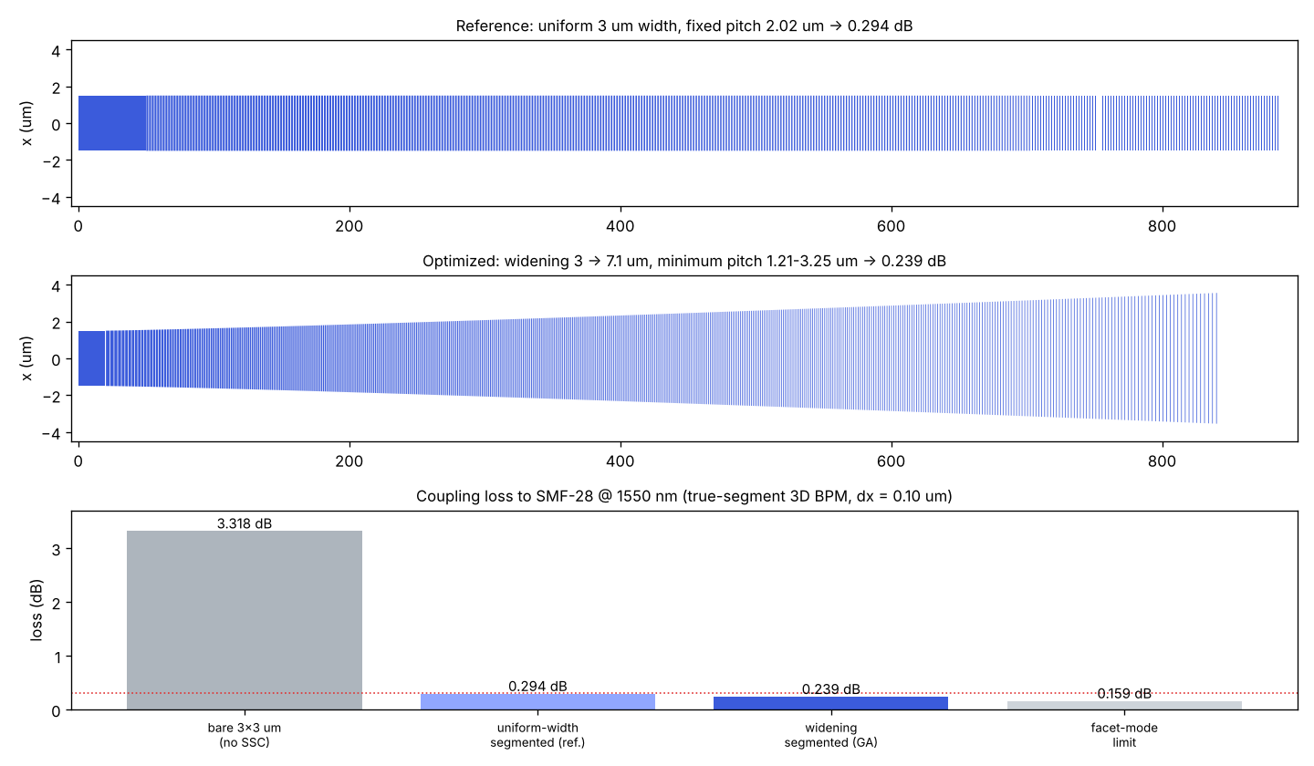
The chip mode (3.9 µm) expands through the widening, thinning segments to ≈ 11.5 × 10.0 µm at the facet. Compared with the earlier uniform-width (3 µm) design with a fixed 2.02 µm pitch (0.294 dB, kept below as the reference), widening the segments lowers the facet-mode limit to 0.159 dB and the dense mid-section pitch keeps the segment radiation small, so the device reaches 0.239 dB.
Tolerance
Condition
Loss
Wavelength
1500 / 1525 / 1575 / 1600 nm
0.243 / 0.237 / 0.251 / 0.268 dB
CD bias (tooth length and width)
−0.10 / −0.05 / +0.05 / +0.10 µm
0.304 / 0.301 / 0.267 / 0.276 dB
Facet cut position
−0.25 µm … +2.0 µm
0.239 – 0.248 dB
SMF offset (x / y)
0.5 µm / 1.0 µm
0.28 / 0.39 – 0.41 dB
GA-optimized SSC — geometry, duty / width ramps, the minimum-pitch rule (tooth and gap ≥ 0.5 µm), GA convergence, top & side |E|² propagation, the facet field against SMF-28, and wavelength / misalignment / fabrication tolerances.Reference uniform-width segmented SSC (fixed pitch 2.02 µm, 0.294 dB) vs. the GA-optimized widening, minimum-pitch geometry (0.239 dB), both on the same dx = 0.10 µm grid.
Method check: a 2D full-wave FDTD of 60 µm segmented sections (pitch 2.0–2.8 µm, duty 0.3–0.75) gives segment losses within −0.06 / +0.02 dB of the paraxial BPM (fdtd2d_calibration.json), so the paraxial BPM is slightly optimistic for segment scattering — a realistic expectation is ≈ 0.24–0.27 dB. The calculation is scalar (polarization-averaged); facet Fresnel reflection is excluded (index-matched butt coupling).
ssc_compare.png — reference vs. optimized comparison figure.
Run with python3 ga_widen.py → python3 verify_widen.py → python3 make_gds_widen.py (needs numpy, scipy, numba, gdstk, matplotlib). The GA takes ≈ 40 min on 2 cores; always re-validate the final candidate on the fine grid (dx ≤ 0.10 µm). The earlier uniform-width study (scripts, solid inverse-taper alternative) is kept in archive_uniform/.