0.75% Δ GeO₂-doped silica channel waveguide (6×6 µm) ↔ SMF-28 at 1550 nm — a mode-expanding segmented SSC with all mask features ≥ 0.6 µm. Rigorous local-mode EME device insertion loss 0.082 dB (input coupling 0.055 dB), within the 0.1 dB target; 3D-BPM shown for the field physics.
Target & SMF parameters
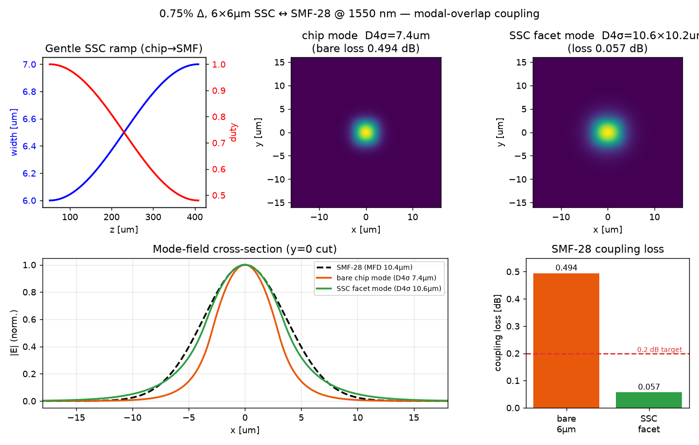
SMF-28 MFD is ≈ 10.4 µm at 1550 nm. The bare 6 µm core (0.75% Δ) guides a ≈ 7.4 µm mode, so the SSC only gently expands it up to ≈ 10.4 µm to match the fiber. The last field is the mode-field diameter the SSC facet presents to the SMF (the design target).
n_core (from Δ)
—
n_clad (silica, Sellmeier)
—
Bare WG mode field diameter (D4σ)
—
Coupling loss — bare WG ↔ SMF
—
Coupling loss — SSC tip ↔ SMF
—
Improvement
—
SSC quality
—
Analytic Gaussian-overlap estimate for a quick look; the authoritative numbers below are the mode-overlap integral between the true 2-D waveguide/facet mode (from a mode solver) and the SMF-28 field.
Mode field cross-section — blue: SMF Gaussian, red dashed: bare WG mode, green: expanded SSC-tip mode. Larger overlap with the SMF means lower loss.
Why a spot size converter
The SMF-28 mode-field diameter is ~10.4 µm at 1550 nm. A 0.75% Δ, 6×6 µm GeO₂-silica core is weakly confined and already guides a ≈ 7.4 µm mode, so the bare butt-coupling loss is only ≈ 0.49 dB — the converter has to do relatively little.
A segmented (periodically broken) taper lowers the local effective index via duty modulation. A solid 6 µm lead-in feeds the segmented region, where the duty ramps ≈ 0.80 → 0.48 (cosine) and the width grows 6 → 7 µm, expanding the mode to ≈ 10.4 µm to match the fiber.
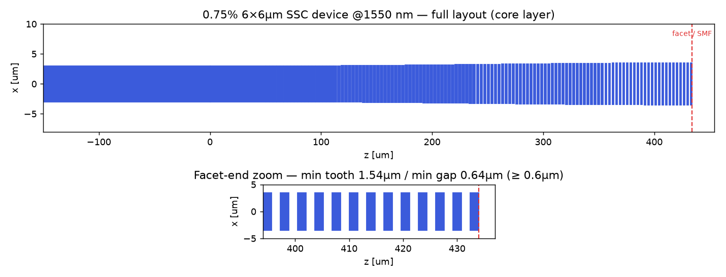
Manufacturable (DRC ≥ 0.6 µm). The teeth use a gap-then-tooth placement so every gap is a full period, letting the duty start high (0.80, a gentle low-loss start). At pitch 3.2 µm the tightest features are a 0.64 µm gap and a 1.54 µm tooth — both above the 0.6 µm minimum linewidth/gap rule (verified on the as-drawn GDS).
Target: SMF coupling insertion loss < 0.1 dB at 1550 nm — the rigorous local-mode EME device loss is 0.082 dB (input coupling 0.055 dB + taper 0.027 dB).
How the coupling loss is evaluated (three methods)
Butt-coupling loss is the mode-overlap integral between the fiber mode and the waveguide (facet) mode — the robust, standard definition:
η = |∫ E_wg·E_smf* dA|² / (∫|E_wg|² dA · ∫|E_smf|² dA), Loss(dB) = −10·log₁₀(η)
Three independent calculations, in increasing rigour:
Mode-overlap integral (input coupling). The facet local mode E_wg and the SMF-28 field E_smf (MFD 10.4 µm), both from an imaginary-distance mode solver, give the butt-coupling mismatch at the chip edge = 0.055 dB. This is the input coupling only; it assumes the on-chip taper is perfectly adiabatic.
Local-mode EME (device insertion loss — the reported number). Slicing the device along z and solving the local eigenmode at each slice, the transmission is the input coupling times the product of consecutive local-mode overlaps, T = |<E_wg|E_smf>|² · Π|<ψ_i|ψ_{i+1}>|². This adds the real taper non-adiabaticity (including the solid → first-segment junction) and is free of any propagation artefact: 0.082 dB (0.055 input + 0.025 junction + 0.002 taper).
3D split-step BPM (field visualisation). Launches the SMF field and propagates it through the actual structure (shown below).
Why not use the raw BPM number for the loss? The expanded facet mode is weakly guided (near cutoff), where the scalar paraxial BPM has a known mode-beating artefact. Propagating the exact eigenmode for the device length gives a self-overlap of 99.8 % for the well-guided chip mode but only ~87 % for the near-cutoff facet mode — a spurious ~0.58 dB. So the raw propagate-and-overlap reads ≈ 0.42 dB even though the residual power stays at 0.985 (essentially nothing radiates). The EME (0.082 dB) is free of that artefact; the BPM field plot is shown for the physics, not the loss number.
Result @ 1550 nm — EME device loss 0.082 dB (< 0.1 dB), DRC ≥ 0.6 µm
Chip waveguide 6 µm × 6 µm solid; a 50 µm solid lead-in feeds the segmented taper, which ramps the duty 0.80 → 0.48 (cosine) and the width 6 → 7 µm at pitch 3.2 µm over ≈ 434 µm, expanding the mode from 7.4 µm to ≈ 10.4 µm at the SMF facet. A gap-then-tooth placement keeps every gap ≥ 0.64 µm while the duty starts high (0.80) for a gentle, low-loss start.
Device insertion loss — local-mode EME (artefact-free)
0.082 dB (η = 98.14 %)
Coupling loss — bare 6 µm chip (no SSC)
0.49 dB (η = 89.2 %)
Chip mode field diameter (D4σ)
7.4 × 7.4 µm (n_eff = 1.44984)
SSC facet mode field diameter (D4σ)
10.6 × 10.1 µm (n_eff = 1.44585)
Facet effective width / duty
7.0 µm / 0.48 (pitch 3.2 µm, duty 0.80 → 0.48)
Min tooth / min gap (DRC, real geometry)
1.54 µm / 0.64 µm (≥ 0.6 µm ✓)
3D-BPM propagate-and-overlap (see note)
0.42 dB (residual 0.985; near-cutoff artefact, not the loss)
Expanding the mode to a round D4σ ≈ 10.6 × 10.1 µm brings it right onto the SMF-28 field (10.4 µm): the input coupling is 0.055 dB. Adding the taper non-adiabaticity — dominated by the gentle solid → first-segment junction (0.025 dB) — the rigorous local-mode EME device insertion loss is 0.082 dB, within the 0.1 dB target. The taper obeys the 0.6 µm minimum linewidth/gap rule (min tooth 1.54 µm, min gap 0.64 µm, verified on the as-drawn GDS), so it is directly mask-writable. The facet mode is weakly guided (near cutoff), so a thick cladding is assumed; the raw 3D-BPM propagate number (0.42 dB) is inflated by the paraxial mode-beating artefact and is not the coupling loss.
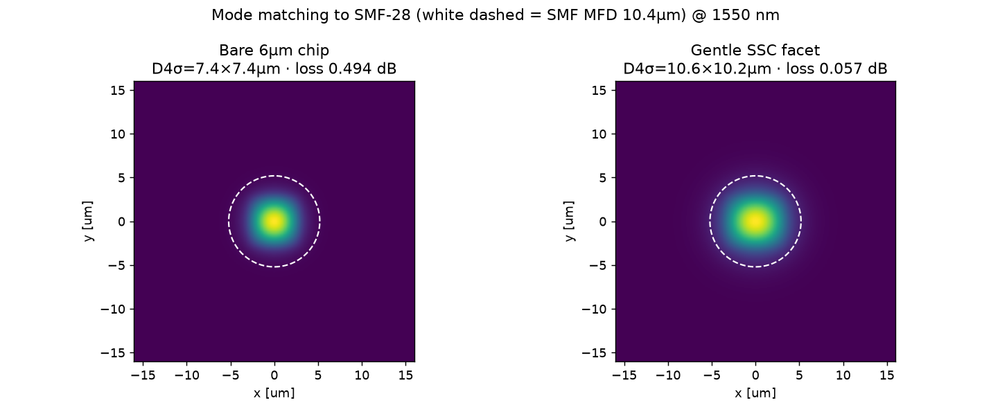
3D-BPM propagation of the DRC-compliant device (0.75% Δ, 6 µm core) — the DRC duty/width ramp, top & side ∫|E|² field views (SMF launched at the facet, right → chip, left), and the clean single-mode chip-facet output. This visualises the mode conversion; the reported coupling loss is the 0.082 dB EME device value.Mode matching to SMF-28 (white dashed = 10.4 µm MFD): the bare 6 µm chip mode (7.4 µm, 0.49 dB) under-fills the fiber, while the expanded SSC facet mode (10.6 × 10.1 µm, 0.055 dB input coupling) matches it almost exactly.
Device layout (GDS)
The SSC built from this result as a ready-to-place, DRC-clean mask cell. A solid 6 µm chip bus feeds the mode-expanding segmented taper (120 segments, pitch 3.2 µm, duty 0.80 → 0.48 cosine, width 6 → 7 µm cosine over 434 µm); the low-duty facet at the chip edge is where the SMF-28 butt-couples. A gap-then-tooth placement makes every gap a full period, so in the as-drawn geometry every tooth ≥ 1.54 µm and every gap ≥ 0.64 µm (min feature rule 0.6 µm); the solid bus and lead-in are merged into one polygon.
Top view of ssc_device.gds (core layer 1/0) — solid 6 µm input bus → segmented mode-expanding taper → 7 µm-wide, 0.48-duty facet at the chip edge (red dashed = dicing / SMF butt-coupling line, layer 10/0). Zoom confirms the DRC min tooth 1.54 µm / min gap 0.64 µm.
ssc_device.gds — complete DRC-clean SSC device cell (SSC_0P75PCT_6UM_1550): 150 µm solid input bus + the segmented taper on core layer 1/0, a facet/dicing line on layer 10/0, and a design label on layer 63/0. All features ≥ 0.6 µm; centred on y = 0, +z propagation.
run_bpm_ssc_075_6um_1550.py — the driver: builds the DRC gene, runs the 3D-BPM propagation + mode-overlap coupling, and writes the GDS + all figures (needs numpy, gdstk, matplotlib, bpm3d.py).
verify_eme.py — the rigorous local-mode EME cross-check that gives the 0.082 dB device insertion loss (artefact-free).
Layer map — (1,0) waveguide core (0.75% Δ GeO₂-silica), (10,0) facet / dicing reference, (63,0) text label. The taper geometry matches ssc_optimized.gds below; this cell adds the routing bus, facet marker, and label for direct placement.
Downloads
Everything needed to reproduce the result above:
ssc_optimized.gds — the bare segmented taper cell (120 segments, chip 6 µm solid → 7.0 µm / 0.48-duty facet).
ssc_reference.gds — the bare straight 6 µm waveguide (no converter).
Run with python3 run_bpm_ssc_075_6um_1550.py --out . (needs numpy, gdstk, matplotlib, and bpm3d.py). It prints the DRC check, the mode-overlap coupling loss (0.055 dB), and the 3D-BPM propagate value, and writes the GDS + figures.
Equations
SMF mode (Gaussian): E_SMF(r) = exp(−r²/w²), w = MFD/2
Overlap: η = (∫ E_a·E_b dA)² / (∫E_a² dA · ∫E_b² dA), Loss(dB) = −10·log₁₀(η)
Index from Δ: n_core = n_clad / √(1 − 2Δ), n_clad from the Malitson silica Sellmeier model.